

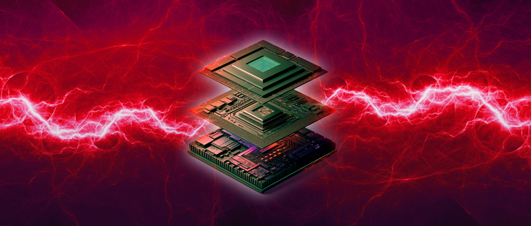
For years, the semiconductor industry had one simple goal: fit more transistors onto a single piece of silicon. This approach gave us faster computers, more powerful smartphones, and increasingly capable gaming consoles. But as manufacturing processes became more advanced, building one massive chip started becoming incredibly expensive, difficult, and inefficient.
Instead of making one giant processor, chipmakers are now taking a different route—building several smaller chips and connecting them together so they function as one. These smaller chips are known as chiplets, and they are transforming the way processors are designed.
From AI accelerators and gaming CPUs to data center processors and automotive systems, chiplets are quickly becoming the foundation of next-generation computing. But what exactly are chiplets, how do they work, and why are companies like AMD, Intel, NVIDIA, and Apple investing heavily in this technology?
Let’s break it down.

Credits: Semiconductor Engineering
What Are Chiplets?
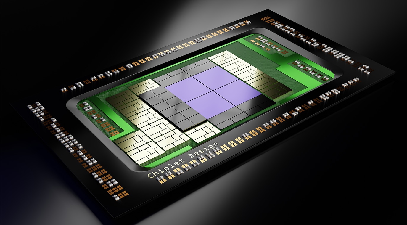
A chiplet is a small semiconductor die that performs a specific function within a larger processor package. Rather than manufacturing every component—CPU cores, graphics engine, memory controller, cache, and input/output circuitry—on one giant silicon chip, manufacturers divide these functions into smaller, specialized dies.
These individual chiplets are then connected using ultra-fast communication links and packaged together so that they behave like a single processor.
Think of it like building a high-performance PC. Instead of soldering every component onto one board permanently, you combine specialized parts such as the CPU, graphics card, RAM, and storage to create a complete system. Chiplets apply a similar philosophy inside a processor package.
Although they are physically separate pieces of silicon, they communicate so quickly that software generally treats them as one chip.
Why the Semiconductor Industry Needed Chiplets
For decades, chipmakers relied on monolithic chip designs, where everything was manufactured on one large silicon die.
This worked well while transistor scaling followed Moore’s Law. However, modern semiconductor manufacturing has become significantly more challenging.
As chips become larger:
- Manufacturing costs increase dramatically.
- Tiny defects can ruin an entire chip.
- Heat becomes harder to manage.
- Designing increasingly complex chips takes longer.
- Moving to new manufacturing nodes becomes more expensive.
Imagine printing an enormous photograph on a single sheet of paper. One small tear or printing defect ruins the entire image. Now imagine printing it in several smaller sections. If one section has a defect, only that part needs replacing.
Chiplets solve a similar problem in semiconductor manufacturing.
How Chiplets Work
Although chiplets are separate pieces of silicon, they operate together inside a single package through extremely fast communication links.
A typical chiplet-based processor consists of multiple specialized components.
CPU Chiplets
These contain the processor cores responsible for running operating systems, applications, and everyday computing tasks.
Manufacturers can simply add more CPU chiplets when higher performance is required instead of designing a completely new processor.
Graphics Chiplets
GPU chiplets handle graphics rendering, AI workloads, and parallel computing tasks.
Future GPUs are increasingly expected to use multiple graphics chiplets to deliver higher performance without creating enormous monolithic dies.
Memory Chiplets
These provide high-speed cache or specialized memory that allows processors to access frequently used data much faster.
Some advanced packaging technologies even stack memory directly above processing chiplets.
I/O Chiplets
These manage communication between the processor and external devices such as SSDs, USB ports, networking hardware, PCIe devices, and system memory.
Separating I/O from compute allows manufacturers to optimize each component independently.
Credits: Tokyo Electron
The Secret Behind Chiplets: High-Speed Interconnects
The biggest challenge with chiplets is making separate silicon dies communicate as if they were one processor.
This is achieved through advanced interconnect technologies.
Instead of traditional motherboard connections, chiplets use microscopic high-speed links capable of transferring enormous amounts of data every second with extremely low latency.
One of the most important emerging standards is Universal Chiplet Interconnect Express (UCIe), which aims to create a common communication language for chiplets from different manufacturers.
The goal is similar to what USB achieved for peripherals—standardization that enables compatibility across the industry.
Without these high-speed interconnects, chiplets would introduce noticeable delays that could hurt processor performance.
Advanced Packaging Makes It Possible
Unlike traditional processors, chiplets rely heavily on advanced packaging technologies.
Instead of simply placing one chip inside a package, manufacturers carefully position multiple chiplets extremely close together.
Some common approaches include:
2.5D Packaging
Multiple chiplets are mounted side by side on a silicon interposer that provides thousands of high-speed connections between them.
This approach is widely used in AI accelerators and high-performance computing.
3D Packaging
Instead of arranging chiplets side by side, manufacturers stack them vertically.
This dramatically shortens communication distances while saving space.
3D stacking also enables technologies such as vertically stacked cache memory, significantly boosting performance without increasing processor size.
Why Chiplets Are Better Than Monolithic Chips
Chiplets aren’t simply a new manufacturing technique—they solve several problems that have become increasingly difficult for traditional chip designs.
Better Manufacturing Yield
Semiconductor manufacturing is never perfect.
The larger a silicon die becomes, the greater the chance that tiny manufacturing defects will render it unusable.
Smaller chiplets have a much higher probability of being defect-free.
Even if one chiplet fails, manufacturers only need to replace that small component instead of discarding an entire expensive processor.
This significantly improves production yields.
Lower Manufacturing Costs
Cutting-edge manufacturing nodes are incredibly expensive.
Not every part of a processor needs to be built using the latest process technology.
For example:
- CPU cores may use a 2 nm or 3 nm process.
- I/O components can continue using an older and cheaper manufacturing node.
- Memory controllers may use another optimized process.
This flexibility reduces manufacturing costs without sacrificing overall performance.
Greater Design Flexibility
Chiplets allow manufacturers to mix and match components like building blocks.
Instead of redesigning an entire processor for every new product, engineers can reuse existing chiplets across multiple processor families.
This modular approach shortens development cycles while reducing engineering effort.
Easier Scalability
Need more processing power?
Instead of creating one massive processor, manufacturers can simply add more compute chiplets.
This approach has already been adopted in modern server processors containing dozens—or even hundreds—of CPU cores.
Scaling performance becomes much more practical.
Improved Power Efficiency
Each chiplet can be independently optimized for power consumption.
Some components may prioritize maximum performance, while others focus on energy efficiency.
Because heat is spread across multiple smaller dies rather than concentrated in one giant chip, thermal management also becomes easier.
Credits: The Indian Express
Heterogeneous Integration: Mixing Different Technologies
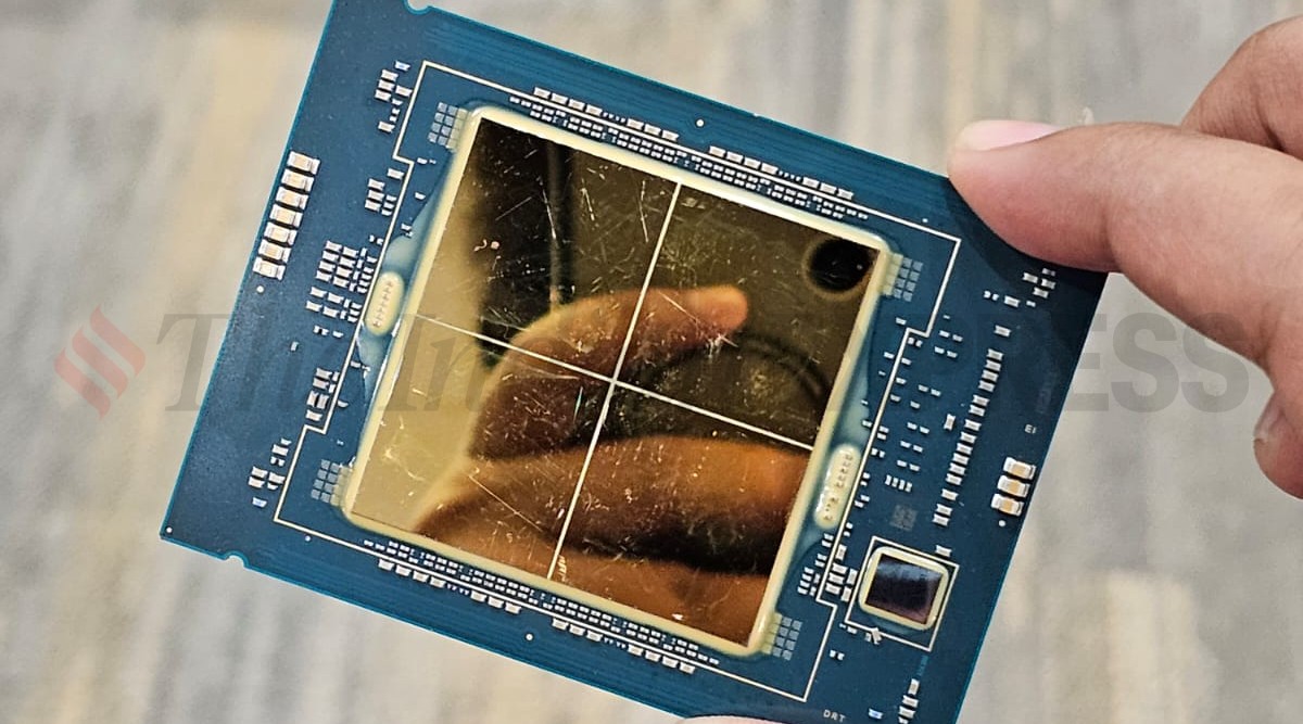
Perhaps the biggest advantage of chiplets is heterogeneous integration.
This means combining different types of silicon built using entirely different manufacturing processes.
For example, one processor package could include:
- High-performance CPU cores
- AI acceleration chiplets
- Graphics chiplets
- Specialized security processors
- Memory chiplets
- Networking chiplets
Each component can be manufactured using the process technology best suited to its specific function.
Previously, all of these elements had to compromise by sharing one manufacturing process.
Real-World Examples of Chiplets
Chiplets are no longer experimental—they’re already powering many of today’s most advanced processors.
AMD was among the first companies to successfully commercialize chiplet-based CPUs with its Ryzen and EPYC processors, separating CPU cores from I/O functionality.
Intel has also embraced multi-die architectures in several modern processors, combining compute, graphics, and specialized accelerators within a single package.
NVIDIA is increasingly using advanced packaging techniques for AI accelerators, while the broader industry is investing heavily in chiplet ecosystems for future GPUs and data center hardware.
Even smartphone and custom silicon manufacturers are exploring modular architectures as packaging technologies continue to improve.
Chiplets have rapidly moved from an emerging concept to a mainstream semiconductor design strategy.
Challenges Chiplets Still Face
Despite their advantages, chiplets are not without challenges.
Communication Overhead
Although interconnects are extremely fast, data still needs to travel between separate pieces of silicon.
If not carefully designed, this can introduce additional latency compared to a fully integrated chip.
Packaging Complexity
Building multiple chiplets into one package requires advanced manufacturing techniques.
Packaging has become almost as important as the chip manufacturing process itself.
This increases engineering complexity and production costs.
Thermal Management
Packing several high-performance chiplets closely together generates significant heat.
Keeping temperatures under control remains a major engineering challenge, particularly for AI processors consuming hundreds of watts.
Standardization
Today, many companies use their own proprietary chiplet technologies.
Industry standards like UCIe aim to create universal compatibility, allowing chiplets from different manufacturers to work together more easily.
However, widespread adoption will take time.

Credits: IDTechEx
The Future of Chiplets
The future of semiconductor design is increasingly modular.
As transistor scaling becomes more expensive and technically challenging, chiplets provide a practical path for continued performance improvements.
Future processors are expected to combine increasingly specialized chiplets, including dedicated AI engines, security modules, networking processors, memory stacks, and domain-specific accelerators.
Advances in 3D packaging, silicon interposers, and optical interconnects could make communication between chiplets even faster, reducing latency to nearly imperceptible levels.
Researchers are also exploring the possibility of creating an ecosystem where companies can purchase standardized chiplets from multiple vendors and assemble custom processors much like selecting PC components today.