


Samsung Electronics and Taiwan Semiconductor Manufacturing Company (TSMC) are intensifying their rivalry in the race to commercialize 2-nanometer (nm) semiconductor technology. With both companies gearing up for mass production next year, this competition is expected to reshape the semiconductor industry. The transition to 2nm chips introduces significant technological challenges, requiring innovative transistor structures and advanced manufacturing processes. Initial yield rates and client acquisitions will be pivotal in determining market dominance.
TSMC appears to have an edge in the 2nm race, thanks to its well-defined timeline and robust client base. The company plans to begin trial production in April 2024, leveraging its multi-project wafer (MPW) service to enable fabless semiconductor companies to test their designs on 2nm technology. Mass production is set for the second half of the year.
Apple, one of TSMC’s largest and most loyal clients, is widely expected to receive the first 2nm chips, likely to power its next-generation iPhones. Other prominent clients, including Advanced Micro Devices (AMD) and Nvidia, are also in line for TSMC’s advanced chips. According to TSMC Chairman Mark Liu, customer demand for 2nm technology has already exceeded expectations, surpassing that for its 3nm process.
To meet this demand, TSMC is rapidly scaling its production capacity, aiming to produce 50,000 wafers per month for the 2nm process. TSMC has also announced a price point of $30,000 per 2nm wafer—double the cost of its 4nm and 5nm wafers—highlighting the premium value of this cutting-edge technology.
Samsung’s Strategic Comeback Under New Leadership
Samsung Electronics, under the leadership of Han Jin-man, is determined to challenge TSMC’s dominance in the foundry market. After setbacks with its 3nm gate-all-around (GAA) process, Samsung is focusing on improving yield rates and fostering strategic partnerships to enhance its competitiveness in the 2nm race.
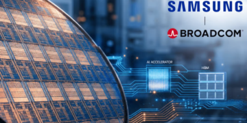
The company has begun converting its S3 foundry line in Hwaseong to accommodate 2nm manufacturing, with test production slated for the first quarter of 2024. Samsung has already secured a key client, Preferred Networks (PFN), a leading Japanese AI startup. Under this partnership, Samsung will produce 2nm-based AI accelerators while offering its advanced 2.5D (I-Cube S) packaging technology. This packaging solution integrates multiple chips into a single package, improving data transmission speeds and reducing overall size.
PFN, supported by major investors such as Toyota, Nippon Telegraph and Telephone Corporation (NTT), and FANUC, represents a significant opportunity for Samsung to establish itself as a leader in the AI-focused semiconductor market.
Technological Challenges of 2nm Transition
The transition to 2nm technology represents a significant leap in semiconductor manufacturing. This process introduces a new transistor structure that enhances performance and energy efficiency but also raises development costs and design complexity.
Key challenges include:
- Improved Wafer Flatness and Atomic Layer Deposition (ALD): Achieving precise bonding and deposition is critical for the successful production of 2nm chips.
- Replacement of 3nm Equipment: Much of the machinery used for 3nm manufacturing must be upgraded or replaced to meet the stringent requirements of 2nm processes.
- Yield Rates: Ensuring high yield rates during initial production is crucial for securing client trust and market share.
Both TSMC and Samsung are investing heavily in research and development to overcome these challenges and ensure reliable production.
Market Implications of 2nm Technology
The 2nm process is expected to revolutionize the semiconductor industry, enabling breakthroughs in artificial intelligence (AI), high-performance computing, and advanced mobile devices. For TSMC, the early production timeline and existing client relationships position it as the frontrunner. Apple’s reliance on TSMC’s 2nm technology for its flagship products underscores the importance of early market entry.
On the other hand, Samsung is banking on its partnerships and advanced packaging solutions to differentiate itself. The contract with PFN highlights Samsung’s strategic pivot toward AI and data-centric applications, which could open new revenue streams and diversify its client base.
The competition between TSMC and Samsung is more than just a technological race; it’s a battle for global foundry leadership. TSMC’s dominance in advanced nodes, backed by consistent yield rates and a strong client base, gives it an edge. However, Samsung’s focus on innovation and its strategic efforts to recover from previous setbacks make it a formidable contender.
As both companies prepare for mass production in 2024, the semiconductor industry is set to witness a transformative shift. The race to 2nm technology will not only determine the future of computing but also redefine the competitive dynamics of the global chip market.

