

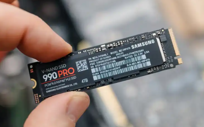
The widespread transition from mechanical hard disk drives (HDDs) to solid-state drives (SSDs) is one of the most significant leaps in consumer and enterprise computing history. By replacing slow, spinning magnetic platters and fragile mechanical read/write heads with non-volatile flash memory, SSDs fundamentally eliminated mechanical friction. Early marketing materials suggested that because these drives contained no moving parts, they were virtually immune to physical wear and would easily outlast traditional systems. However, as flash storage scales to higher capacities and handles heavier computing workloads, the reality has proven far more complex. The long-term durability of modern flash drives is shaped by a definitive bottleneck; investigating why SSD health declines reveals a complex interaction of quantum physics, internal management inefficiencies, and environmental stresses that gradually wear down the drive’s microscopic cells.
Unlike mechanical drives, which typically fail due to motor wear or physical head crashes, an SSD possesses a finite lifespan dictated by the chemical and electrical limits of its underlying silicon. Every time you save a document, download an update, or run an application, the drive undergoes microscopic structural changes. Compounded by complex background processes like garbage collection and aggressive write amplification, this continuous use causes the hardware to lose efficiency over time. Understanding these internal wear mechanisms is essential for anyone looking to protect critical data pipelines, manage high-density enterprise servers, or maximize the lifespan of their daily personal storage systems.
1. The Quantum Core: The Physics of NAND Flash Degradation
To understand the core reasons behind the decline of solid-state storage health, one must shrink down past the plastic casing and explore the subatomic environment of the NAND flash memory cell. Modern solid-state storage saves data by trapping electrons inside microscopic microscopic structures known as floating gate transistors or charge trap cells.
Fowler-Nordheim Tunneling and Oxide Degradation
To alter the state of a memory cell from a binary 1 to a binary 0, the SSD controller must push electrons through an ultra-thin insulating layer made of silicon dioxide (SiO2). This layer acts as a physical wall surrounding the floating gate. The drive triggers this movement by applying a high voltage (15V to 20V) across the control gate. This strong electrical field forces the electrons to snap straight through the insulating barrier via a quantum mechanics phenomenon known as Fowler-Nordheim Tunneling.
While this quantum tunneling mechanism allows for fast, non-volatile data storage without moving parts, the intense high-voltage pushes cause microscopic chemical wear. Every single Program/Erase (P/E) cycle cracks and strains the atomic layout of the oxide insulator. Over thousands of write cycles, this continuous electrical stress creates permanent atomic fractures within the dielectric wall.
Electron Trapping and Cell Blur
As the insulating layer degrades, two distinct, destructive failure modes emerge inside the flash memory structure:
- Charge Leakage: The structural cracks in the oxide wall allow trapped electrons to slowly leak out of the floating gate and escape back into the channel, causing the cell to lose its charge over time and corrupting the stored data.
- Unintentional Electron Trapping: Stray electrons become permanently wedged inside the fractured oxide layer itself.
When the quantity of these permanently trapped, unintentional electrons creates a residual electric field large enough to obscure the intentional charge, the SSD controller can no longer reliably tell the difference between a binary 1 and a 0. At this stage, the cell is officially considered worn out and must be retired, directly lowering the drive’s reported health status.
2. The Multi-Bit Trap: The Vulnerability of MLC, TLC, and QLC Architectures
The underlying structural decline of flash memory cells has been significantly accelerated by the storage industry’s ongoing push to maximize storage density while lowering manufacturing costs.
The Evolution of Cell Storage Density
| Flash Cell Structural Class | Bits Stored Per Cell | Distinct Voltage States Required | Typical P/E Cycle Endurance Lifespan |
| SLC (Single-Level Cell) | 1 Bit | 2 Volts (00, 01) | 90,000 to 100,000 Cycles |
| MLC (Multi-Level Cell) | 2 Bits | 4 Volts (00, 01, 10, 11) | 10,000 Cycles |
| TLC (Triple-Level Cell) | 3 Bits | 8 Volts (000 through 111) | 3,000 Cycles |
| QLC (Quad-Level Cell) | 4 Bits | 16 Volts (0000 through 1111) | 500 to 1,000 Cycles |
The Shrinking Margin of Error
When the solid-state industry relied primarily on Single-Level Cell (SLC) flash memory, a cell only needed to distinguish between two distinct electrical states: charged or uncharged. Even if the oxide layer suffered moderate structural wear, the raw gap between the two voltage states was massive, allowing the controller to easily determine the correct binary value.
However, modern consumer drives rely heavily on Triple-Level Cell (TLC) and Quad-Level Cell (QLC) architectures. A QLC cell must split its small capacity to hold 16 distinct voltage levels. This means the margin of error between different binary states is incredibly tight. Even minimal electron trapping or slight charge leakage will shift the cell’s voltage signature into a neighboring state, triggering a read error. As a result, QLC cells can only survive a fraction of the write cycles that older SLC designs endured before failing.
3. The Management Tax: Write Amplification and Garbage Collection
The physical decline of flash memory is further aggravated by a fundamental operational limitation: the drive cannot overwrite existing data on the fly.
The Block/Page Mismatch
NAND flash memory is organized into a highly rigid structural layout. Storage space is divided into large Blocks, which are further broken down into individual Pages. While the drive can read and write data at the small Page level (typically 4KB to 16KB), it can only execute an erase command across an entire large Block (typically 2MB to 4MB).
When you modify a file, the drive cannot simply overwrite the existing pages. Instead, the SSD controller must find an empty block, copy the unaltered data from the old block alongside your new changes, and then wipe the entire original block to prepare it for future writes. This background optimization process is known as Garbage Collection.
The Cost of Write Amplification
This structural mismatch triggers a destructive phenomenon known as the Write Amplification Factor (WAF). If a user tries to save a tiny 4KB file, the background garbage collection process may be forced to read, move, and rewrite an entire 4MB block of data to complete the task.
In this scenario, the drive performs significantly more physical write operations than the host operating system requested. A high WAF multiplies the real-world wear on the drive’s silicon, consuming the drive’s rated Terabytes Written (TBW) lifecycle threshold much faster than expected and causing its overall health to drop prematurely.
[Image diagram showing the block erase vs page write conflict leading to write amplification]
4. Environmental Catalysts: Thermal Variance and Power Failures
While structural write cycles represent the primary driver of flash decay, external environmental factors play a major role in accelerating component failure.
The Thermal Paradox
Heat impacts an SSD in two completely opposing ways, depending on whether the drive is actively processing data or sitting idle in storage:
- Active Operation: When the drive is actively writing data, higher temperatures (60 °C to 70 °C) actually reduce wear on the silicon. The heat gives the electrons higher kinetic energy, allowing them to tunnel through the oxide barrier cleanly without becoming permanently trapped.
- Idle Storage: When the drive is powered down for archival storage, high temperatures are highly destructive. If a worn drive is stored in a hot environment (50 °C to 80 °C), the thermal energy accelerates electron leakage out of the floating gates, causing the drive to lose its stored data within months or weeks.
Electrical Power Surges
Because solid-state storage relies on managing precise electrical charges across millions of microscopic transistors, sudden voltage fluctuations present a major risk. A sudden power loss or spike can easily corrupt active data caches or cause permanent damage to the delicate internal controller chip, rendering the entire drive unreadable long before its memory cells hit their physical wear limits.
Strategic Playbook: Mitigating the Decline of Solid-State Media
To counter this inevitable physical degradation, modern drives employ automated, internal maintenance tools built directly into their firmware:
- Wear Leveling Algorithms: The drive controller continuously monitors the erase counts of all blocks, actively routing new writes away from heavily used sections toward fresher cells to ensure the entire drive wears down evenly.
- Over-Provisioning Buffers: High-quality manufacturers reserve an extra pool of unlisted storage cells (typically 10% to 20% of the drive’s total capacity). These hidden blocks are kept completely out of reach of the user, allowing the controller to seamlessly swap them in to replace dying cells over time.
For everyday users looking to optimize their drive’s lifespan, the best defense is preserving a solid buffer of free space keeping 20% to 30% of the drive empty ensures the internal garbage collection systems can run efficiently, keeping the Write Amplification Factor low and extending the performance life of the silicon.


