

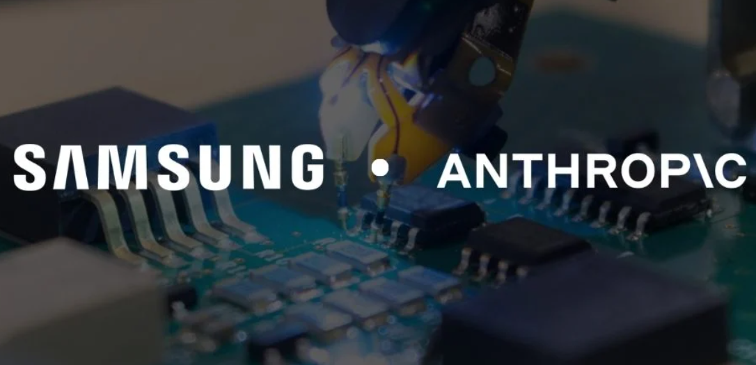
The hyper-competitive frontier of artificial intelligence has officially moved past algorithmic tweaks into a high-stakes race for custom hardware ownership. For the past several years, elite Silicon Valley research labs have operated at the mercy of intense hardware shortages and rigid ecosystem locks, standardizing their massive model training pipelines almost exclusively on expensive general-purpose processors. However, as the economics of serving millions of daily queries become increasingly unsustainable, the world’s leading labs are scrambling to take direct control of their internal supply lines. According to an explosive investigative report from The Information, Anthropic has initiated early-stage development of its own silicon architecture. To bring this project to life, the software lab is pursuing an aggressive in-house AI chip project in partnership with South Korean manufacturing giant Samsung Electronics.
The preliminary talks mark a massive strategic escalation in Anthropic’s long-term hardware roadmap. While the San Francisco-based startup has publicly maintained that its deeply entrenched cloud infrastructure partnerships with Google and Amazon will remain central to its immediate compute footprint, its massive financial scaling has changed the math. Having recently achieved an annualized revenue run rate passing $30 billion, Anthropic now possesses the immense capital reserves required to fund expensive bespoke hardware development. By courting Samsung’s cutting-edge foundry division, the developer of the Claude model is attempting to secure an independent operational runway, insulating its future software iterations from the pricing power and shipment backlogs of traditional hardware suppliers.
1. The Engineering Playbook: Shifting from Exploration to Active Blueprints
While industry rumors surrounding Anthropic’s hardware ambitions have floated for months, the firm’s recent high-level personnel moves prove that its in-house AI chip project has advanced into an active development phase. The most definitive signal of this operational shift arrived with Anthropic’s recent recruitment of Clive Chan, a highly respected semiconductor architect who previously served as a foundational engineer for OpenAI’s dedicated custom silicon division.
Chan’s arrival gives Anthropic the technical leadership needed to coordinate complex chip layout designs. Rather than relying on basic off-the-shelf reference designs, Chan’s team is actively exploring ways to leverage Samsung’s upcoming 2-nanometer (nm) Gate-All-Around (GAA) manufacturing process. This ultra-fine node shrinks transistor dimensions to microscopic boundaries, maximizing raw processing power while dramatically reducing the real-time electrical draw of high-density server superpods.
2. The Packaging Premium: Eliminating the Memory Bottleneck
The decision to choose Samsung over other contract foundries extends far beyond standard wafer fabrication, wrapping in a critical engineering advantage known as advanced packaging.
Semiconductor Sourcing Architecture and Alliance Projections
| Sourcing Alignment Pillar | Traditional Silicon Sourcing Models | Anthropic’s Strategic Samsung Synergy |
| Foundry Node Target | Highly constrained 3nm / 4nm lines | Advanced 2-Nanometer GAA Layouts |
| Packaging Architecture | Fragmented multi-vendor supply paths | Turnkey I-Cube / H-Cube logic integration |
| Memory Buffer Layers | Open-market commodity HBM bids | Direct integration of next-gen HBM4 modules |
| Supply Chain Autonomy | Total reliance on single-foundry slots | Diversified manufacturing with sovereign backing |
In modern artificial intelligence computing, processing power alone is no longer the primary performance ceiling; the true barrier is memory bandwidth. When an advanced model processes a massive multi-modal query, the system frequently stalls while waiting for data to travel between the core logic processor and the neighboring High-Bandwidth Memory (HBM) modules.
Samsung provides a unique structural advantage as the only global player capable of delivering a complete, in-house turnkey solution. By managing the logic chip fabrication, manufacturing the underlying HBM4 memory stacks, and binding them together on a single microscopic substrate using advanced packaging technology, Samsung can eliminate these data bottlenecks while protecting Anthropic from multi-vendor manufacturing delays.
3. The Oligopoly Fracture: Matching the Moves of Silicon Rivals
Anthropic’s push into custom hardware design is a necessary defensive move within a rapidly changing industry, mirroring similar high-profile shifts executed by its primary commercial rivals. Just weeks prior to this disclosure, arch-rival OpenAI unveiled its first custom-designed silicon asset, an inference-optimized processor built in collaboration with Broadcom under the internal codename “Jalapeño.” Simultaneously, hyperscalers like Amazon (Trainium), Google (TPU v5p), and Meta (MTIA) are aggressively packing their data centers with custom application-specific integrated circuits (ASICs) to slash their operational costs.
Because serving real-time chat responses to millions of users after a model is trained is far more expensive than the initial training phase, building an in-house inference accelerator gives Anthropic a critical financial lever, allowing it to dramatically drop the cost of running autonomous enterprise agents.
The Strategic Macro Rebalance
The preliminary talks have already sent massive ripples through the global financial markets. News of the potential alliance triggered an immediate, dramatic single-session reversal on the Seoul stock exchange, driving Samsung’s stock up by 8.22% as global investors welcomed the prospect of the foundry securing a flagship Silicon Valley client to challenge TSMC’s global market dominance.
While the project remains in its infancy and a final contract has yet to be finalized, Anthropic’s aggressive entry into custom hardware design signals an unmistakable industry reality: the world’s leading artificial intelligence labs are no longer content being software developers. To survive a high-stakes war of attrition, they are transforming into full-scale hardware architects, ensuring that the next generation of digital intelligence is fully optimized from the underlying atomic silicon up.


