


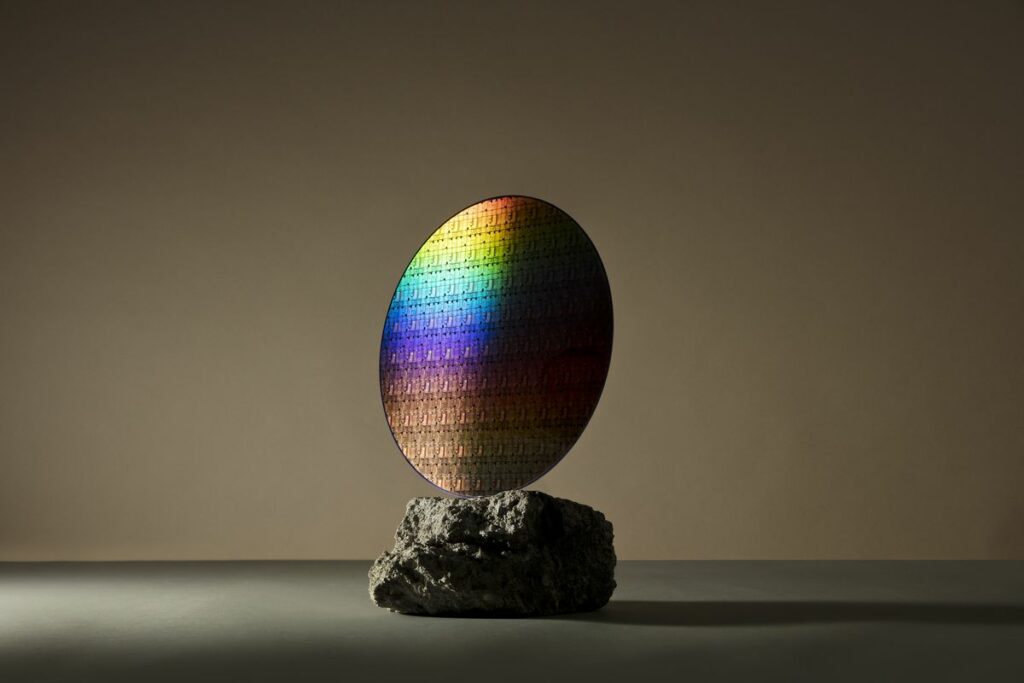
IBM and Samsung have developed a novel way to stack transistors vertically on a chip, which they call “vertical stack” (instead of lying flat on the surface of the semiconductor).
The new Vertical Transport Field Effect Transistors (VTFET) architecture is intended to replace the current FinFET technology, which is utilised in some of today’s most advanced circuits, and could allow for even more densely packed transistors than are currently possible.
In essence, the new design stacks transistors vertically, allowing current to flow up and down the stack rather than the current-flowing side-to-side horizontal architecture found on most chips.
Vertical semiconductor designs have been popular for a time (FinFET already provides some of these benefits); Intel’s future roadmap appears to follow suit, but its initial efforts concentrated on stacking chip components rather than individual transistors. After all, after you’ve exhausted all other options for cramming more chips into a single plane, the only place to go is up (apart from literally reducing transistor technology).
While VTFET designs are still a ways off from being used in consumer circuits, the two businesses are making some bold claims, claiming that VTFET chips may provide a “two-fold gain in performance or an 85 percent reduction in energy use” over FinFET designs.
VTFET technology, IBM and Samsung argue, might help maintain Moore’s law’s goal of continually growing transistor count moving forward by squeezing more transistors into processors.
IBM and Samsung are also speculating on some far-fetched applications for the new technology, including “cell phone batteries that could go over a week without being charged, instead of days,” “less energy-intensive cryptocurrency mining or data encryption,” and “even more powerful IoT devices or even spacecraft.”
Earlier this year, IBM unveiled their first 2nm chip, which takes a different approach to packing more transistors onto a circuit by scaling up the amount that can be placed onto a chip using the existing FinFET design.
VTFET, on the other hand, would try to go much further, though it would likely be even longer before we see chips based on IBM and Samsung’s latest technology on the market.
It isn’t the only corporation looking ahead to the future of manufacturing. Over the summer, Intel unveiled their forthcoming RibbonFET (Intel’s first gate-all-around transistor) design, which is set to be part of the Intel 20A series of semiconductor products, which is scheduled to begin scaling production in 2024.
In addition, the business has unveiled its own concept for stacked transistor technology as a potential RibbonFET successor in the future.


