

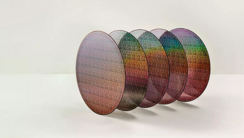
Image Credits: IBM
IBM and Samsung have unveiled a semiconductor design breakthrough that might lay the groundwork for powerful new computers with higher transistor density than ever before. The pair presented research into the novel architecture that sets transistors perpendicular to the surface of the chip, with vertical current flow in both directions, at the annual IEDM semiconductor conference.
The chip architecture is known as a VTFET, which stands for vertical transport field-effect transistor. The unique technique, according to IBM and Samsung, offers a clear route to scaling beyond nanosheet manufacturing technology, after which the spacing between transistors on a chip drops to less than 1nm (for context, a strand of human DNA is 2.5nm in diameter).
“Today’s technological announcement is about pushing convention and reimagining how we continue to develop society and offer new technologies that enhance life and lessen our environmental footprint,” said Dr. Mukesh Khare, Vice President of Hybrid Cloud and Systems at IBM Research.
“In light of the industry’s existing restrictions on numerous fronts, IBM and Samsung are proving our commitment to cooperative innovation in semiconductor design and a shared pursuit of what we call ‘hard tech.'”
Newly Designed Chip for Smartphones
Today’s most prevalent chip topologies are referred to as lateral-transport field-effect transistors (or FETs). Transistors, for example, are packed onto the surface of a chip in fin field-effect transistor (finFET) design, with current flowing sideways between them. Engineers, on the other hand, have an additional dimension to work with VTFETs, as current flows both upward and downward.
“Previously, designers squeezed more transistors onto a chip by decreasing its gate pitch and wire pitch,” IBM noted. “However, even with the most modern finFET technology, spacers, gates, and contacts are limited.”
“[VTFET] overcomes scaling hurdles by loosening physical limits on transistor gate length, spacer thickness, and contact size, allowing these properties to be tailored for performance or energy consumption.”
According to IBM, this achievement is noteworthy for two key reasons. For starters, VTFET is predicted to pave the way for the continuance of Moore’s Law (a 1965 forecast that the number of transistors on a device will double every year), something many felt was unachievable. Of course, the more transistors there are, the more powerful the chip – and hence the computer, workstation, server, and so on.
Second, VTFETs is supposed to allow for more current flow with less wasted energy, potentially reducing chip energy consumption by up to 85 percent when compared to standard FETs. In terms of real-world implications, IBM claims that chips based on VTFET design might pave the way for smartphones with more than a week’s battery life, substantially lower the energy required to conduct compute-intensive activities (such as crypto mining and data encryption), and more.


