

Image Credits: Gizbot
The majority of high-end mainstream CPUs and GPUs continue to use a single chip. While increasing the size of the chip to improve the performance of these processors is possible. However, fabbing larger-sized chips reduces yield rate since a single mistake might render the chip utterly worthless.
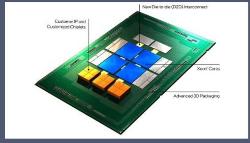
Details about Chiplet
This is why companies like AMD and Intel are looking forward to developing and constructing chiplets, which are nothing more than a pair of processors that function in tandem with one another. This enables the corporation to produce a huge number of little chips while reaping the benefits of a single large chip or processor.
To achieve die-to-die connections, Intel is adopting Universal Chiplet Interconnect Express (UCIe) requirements, which are an open industry standard. This enables the chiplets to communicate at rapid rates with one another. Currently, the UCIe 1.0 provides 20 times faster I/O performance while consuming 1/20th the power of an off-package SerDes.
Intel has recently developed an IFS (Intel Foundry Services) open chiplet platform that enables clients to obtain CPUs with flexible design. Customers will be able to obtain a system-on-package rather than a system-on-chip, which will include modular blocks of semiconductors known as chiplets.
Applications for chiplets
According to Intel, chiplet design may be employed for data center CPUs, particularly for those seeking customised computing machines with increased performance and the ability to handle current workloads such as AI-related jobs.
A CPU built on modular chiplets can have numerous CPU chips, memory chips, and customized chips to fulfill a variety of functions. A chiplet can also include on-package memory, allowing customers to create bespoke solutions for data center applications.
When compared to off-package connections, this also provides high-bandwidth memory access. This will be comparable to the Apple Silicon, which likewise has an embedded memory that is not user-upgradable. It should be noted, however, that the Apple Silicon M1 is not a chiplet, but rather a single chip with integrated memory.
Advanced packaging employs technologies such as the multi-die interconnect bridge (EMIB), which provides high-density on-package interconnection of heterogeneous chiplets with only a tiny bridge die and numerous routing layers. Chiplets will enable Intel IFS clients to tailor a CPU to their specific requirements, ensuring that it is both efficient and powerful.


